Synchronous
Modulator
Versions 1 and 2 |
All materials
and content contained on this page are the exclusive intellectual property of
Andrew R.
Morris and
may not be copied, reproduced, distributed or displayed without his express written
permission. |
|
|
|
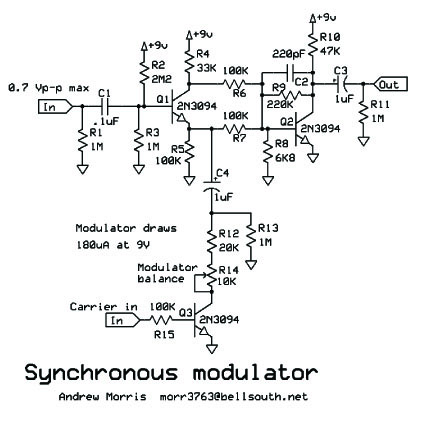
This unique circuit uses a very small amount
of battery current and has excellent carrier suppression. Its only shortcoming is
that you must limit the input signal to 0.7 Vp-p in order to prevent distortion. To
use higher input voltages, replace Q3 with a JFET. A MOSFET doesn't do as well as an
NPN transistor. |
| More:
Operational Amplifiers;
Modulators |
| Click on the Schematics to
view PDFs Version 1 |
 |
|
|
Version 2 |
|
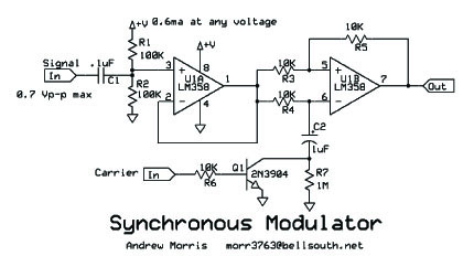
This is an opamp version of the above circuit. It has
more consistent performance over varying power supply voltage than the discrete version,
but it still has the 0.7 Vp-p limitation of the maximum input voltage. You should
use a JFET or a CMOS
switch in place of Q1 if you need to accommodate a high input
voltage. Also a low pass filter needs to be adder after the output of the circuit,
where the discrete version had one built in. |
 |
|
Got Designs?
Please eMail if you want me to link to and/or post your original design. Thanks. |
|
|