|
 |
Circuits designed by David Johnson,
P.E.
Last Updated on:
Saturday, December 23, 2017 02:27 PM
List of Dave's Circuit Designs
The contents & graphics of
Discovercircuits.com are copyright protected.
LINKING to Dave's circuits is permitted but DO NOT COPY any files to your WEB
SITE server |
|
|
|
More
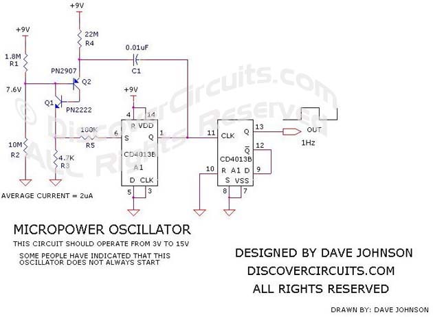
Astable Oscillator Ultra Low Current Oscillator #4
-- January 28, 2010 The circuit below was
inspired by a programmable unjunction transistor (PUJT) circuit sent to me by Karl
Isbrecht. In Karl’s circuit, the unijunction circuit made click sounds in a
speaker and consumed very little power. His circuit reminded me that a PUJT
circuit could be made using a couple common transistors wired in a configuration
like a SCR. In the circuit below, the output of the two transistor pulse
generator is connected to a CD4013 dual flip/flop. One flip/flop is
configured as a non-inverting buffer. The second is wired as conventional
divide by two counter. The result is a nice low frequency square wave
generator, which draws only 2ua from a 9v supply. The circuit will also work
with a DC supply voltage ranging from 3v to 15v. |
|
| The circuit
below was inspired by a programmable unjunction transistor (PUJT) circuit sent to me
by Karl Isbrecht. In Karl’s circuit, the unijunction circuit made click sounds
in a speaker and consumed very little power. His circuit reminded me that a PUJT
circuit could be made using a couple common transistors wired in a configuration like
a SCR. In the circuit below, the output of the two transistor pulse generator is
connected to a CD4013 dual flip/flop. One flip/flop is configured as a
non-inverting buffer. The second is wired as conventional divide by two counter.
The result is a nice low frequency square wave generator, which draws only 2ua from a
9v supply. The circuit will also work with a DC supply voltage ranging from 3v
to 15v. |
| The two transistor
pulse generator circuit is biased to about the ľ supply level. A high value
resistor is used to charge up a small capacitor. When the capacitor reaches
a voltage slightly above the bias voltage, the PNP transistor starts to conduct.
Current from that part is fed to the base of the second NPN transistor.
The collector of the second transistor is
connected to the base of the PNP, so the second NPN transistor turns on the PNP
transistor even harder. This current feedback causes the circuit to quickly
snap into full conduction, which results in the discharge of the capacitor into
the resistor R3. The voltage that appears at R3 is connected to the set
input of the CD4013. With the configuration shown, the voltage at R3
produces a similar voltage at the Q output. |
|
|
| The Q output
is connected to the charging capacitor, so the capacitor is discharged and charged up
slightly negative. The positive feedback aids in maintaining oscillation.
The output of the first half of the CD4013 is connected to the other half. That
side is configured as a classic divide by two counter. So, each pulse produced
by the oscillator produces a state change in the flip/flop. With the component
values shown, the circuit produces a very clear 1Hz square wave signal. |
| |
|
Click on Drawing Below to view PDF version of Schematic |
|
 |
|
|
|
|