|
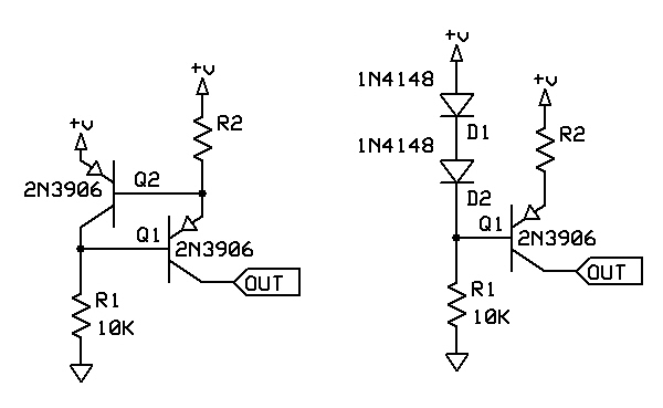
R1 is extremely
non-critical. Its purpose is to limit the current through Q2 or D1 and D2 to reasonable
levels with the particular voltage source; in this case, 9 volts. The current through R1
needs to be at least the current through R2 divide by the minimum beta of Q1 which is
100. I'd add a little extra current to keep some current flowing in D1 and D2 or Q2. For
example, the maximum resistance for R1 in this case would be calculated as follows:
Assume +V is 9V,
and the desired current limit is 6ma.
Voltage drop
across R1 is 91.2 or 7.8 volts.
Base current of
Q1 (and minimum current through R1) is 6mA (desired current limit) divided by 100 equals
0.06mA. I would add an extra 1mA to ensure proper operation of Q1 or D1 and D2. To
calculate R1 would be 7.8 divide by 1.06ma or 7.36K. The nearest standard lower value is
6.8K. If the 9V power supply is going to vary (such as a battery), use the minimum
usable battery voltage in your calculations.
Q1 in the first
circuit may be replaced with a MOSFET, allowing an extremely high value for R1, such as
1 megohm. In this case, R1 can be as high as possible that will not be sensitive to
interference, or reduce the frequency response below requirements. A MOSFET for Q1 is
most attractive at high current levels, because current through R1 can be a big waste of
power if Q1 is a bipolar transistor. |